Memory‑Bound Inference: Why High‑Bandwidth Memory, Not FLOPs, Sets the Pace in AI – and What That Means for Blackwell vs. TPUs
It’s sunday night and NeurIPS is over. The Reagan National Defense Forum is over, and I’m sitting here in Fort Worth marinating in FOMO tracking the news from the weekend. Instead of live hallway conversations in San Diego or Simi Valley, my consolation prize is to deep dive into the hardware details that actually drive inference throughput. If Google is right that modern LLM inference is fundamentally High Bandwidth Memory (HBM)-bound, not FLOP-bound, then everything from how we value accelerators to how we think about “AI infrastructure” is subtly wrong—and that shift shows up very concretely in Blackwell’s bandwidth-first design and the walls TPUs are starting to hit.
At DARPA and Lockheed, I had to manage lots of various microelectronics programs and I’m really interested in how the economics of Google, Amazon, Tesla, Intel? and others are going to try to eat away at NVIDIA’s market share. My conclusion? This market share is not simple to grab and NVIDIA’s moat may actually be widening. This post reflects my personal views only and is not investment advice, and I am not a current professional expert in semiconductor or AI hardware equity analysis, so please do your own research before making any financial decisions.
Big programs and complex systems like the F-35 or the Boeing 737 live or die by the velocity of their supply chains. Good management is constantly obsessing over the theory of constraints as articulated by Goldratt. It’s helpful to look at a system and understand where the scarcity and abundance are and will be and then understand the drivers over time that will be the next gate you have to worry about.
Large language models (LLMs) and their transformer-based architecture have shifted the centre of gravity in AI hardware. A recent comment on X pointed out that if inference is truly HBM‑bound (as Google engineers themselves suggest), then the market has been modeling throughput incorrectly. This post dives into the technical reasons why floating point operations (FLOPs) alone don’t determine inference performance, explains why the industry’s “memory wall” has become the limiting factor, and examines how NVIDIA’s Blackwell architecture is designed around bandwidth and locality while even the newest TPU variants still struggle against the memory bottleneck.
The physics: compute scales faster than memory
Semiconductor scaling has delivered exponential growth in raw compute power, but memory capacity and bandwidth have lagged. An academic review of the “memory wall” notes that peak server FLOPS have been scaling roughly 3× every two years, whereas DRAM and interconnect bandwidth grow only ~1.6× and 1.4×, respectively. This divergence means that transferring data to the compute units is increasingly the bottleneck. The review argues that for many AI workloads the time to complete an operation is completely limited by DRAM bandwidth; no matter how fast arithmetic units are, they starve if data cannot be fed quickly.
Google’s infrastructure engineers echo this warning. Amin Vahdat wrote that advances in AI require redesigning the compute backbone because performance gains in computation have outpaced growth in memory bandwidth; simply adding compute units will cause them to idle while waiting for data. The first‑generation TPU design illustrates the point: Google admitted it was limited by memory bandwidth, so the second generation switched to High‑Bandwidth Memory (HBM) to increase bandwidth to 600 GB/s and double performance.
Why LLM inference is memory‑bandwidth bound
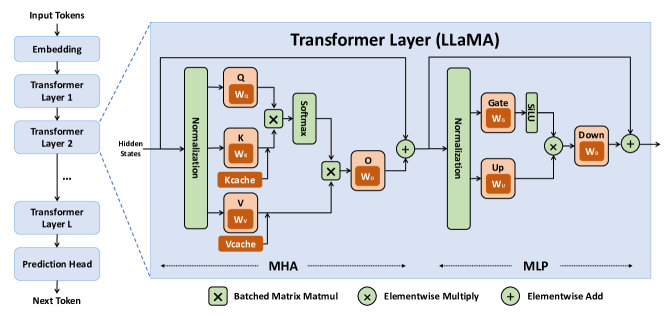
During LLM training, large batches reuse weights across many tokens, so arithmetic intensity is high and compute FLOPs dominate. Inference is different. Each token’s generation (decode) must fetch model weights and the per‑token key–value (KV) cache from HBM and write back updated KV states. A widely read technical guide shows that during generation, the arithmetic intensity of the attention block collapses: we perform a tiny matrix–vector multiply while streaming the entire KV cache. As a result we are basically always memory bandwidth‑bound during attention. The guide further notes that every sequence has its own KV cache, so larger batch sizes only increase memory traffic; we will almost always be memory‑bound unless architectures change. In concrete numbers, serving a 30B parameter model on a 4×4 TPU v5e slice (8.1 TB/s aggregate HBM bandwidth) yields a lower‑bound step time of 2.5 ms for a batch of four tokens, dominated by loading the weights and KV cache.
SemiAnalysis provides a similar picture. They explain that LLM inference repeatedly reads model weights and the KV cache from HBM and writes back the new key–value, and if bandwidth is insufficient, compute units sit idle. Consequently, most inference workloads are memory‑bandwidth bound. The report warns that increasing on‑chip FLOPs or even adding more HBM stacks does not eliminate the bottleneck because models expand to consume available memory (a “memory‑Parkinson” dynamic).
Even at the operator level, GPU microbenchmarks show that operations such as layer normalization, activations and attention remain HBM‑bound until sequence lengths of 4–16k tokens. AMD’s MI300X white paper likewise notes that many inference operations stay bandwidth‑limited until extremely large batches are used.
FLOPs versus memory bandwidth
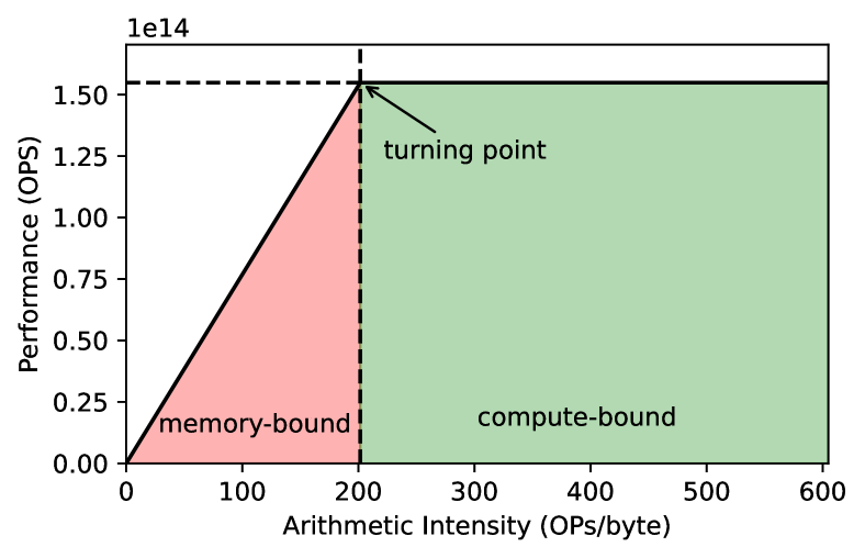
In TPUs, each TensorCore contains a large matrix‑multiply unit (MXU), a vector unit and a very small on‑chip scratchpad (VMEM). Data must be copied from off‑chip HBM into VMEM before computation. The bandwidth between HBM and the TensorCore (typically 1–2 TB/s) limits how fast computation can be done in memory‑bound workloads. For matrix multiply operations (matmuls), the TPU architecture overlaps HBM loads with compute so that weight loads can be hidden, but for attention blocks this is not possible. When the load from HBM to VMEM is slower than the FLOPs in the MXU, the operation becomes bandwidth bound. Thus, adding more FLOPs does not improve throughput once the memory system is saturated.
These insights are why many accelerator researchers use arithmetic intensity (FLOPs per byte transferred) to model performance. For most LLM decode workloads the arithmetic intensity is low, so the throughput is proportional to the available memory bandwidth rather than the peak FLOPs. SemiAnalysis quantifies this: the MI300X, despite delivering over 5 PFLOPs of FP8 compute, is HBM‑bound for real‑world sequence lengths; the compute units simply cannot be saturated.
Evidence from Google: memory-optimized inference
Google’s own authors repeatedly acknowledge that inference is memory‑limited. The incredible DeepMind “How to Scale Your Model” (read it) series emphasizes that during generation, the attention block’s arithmetic intensity is constant and low; we’re doing a tiny amount of FLOPs while loading a massive KV cache. They advise that increasing batch size yields diminishing returns because each extra sequence adds its own KV cache. In follow‑up chapters describing Llama 3 inference on TPUs, the authors derive a 2.5 ms per‑step lower bound solely from HBM reads and note that for large KV caches we are well into the memory‑bound regime. When the KV cache fits into on‑chip VMEM, the decoder becomes compute‑bound, but in realistic models this rarely happens.
Google’s hardware roadmap also priotizes memory. The Ironwood TPU (v7) is marketed as “the first TPU for the age of inference.” In its technical brief, Google states that LLMs, Mixture‑of‑Experts and “thinking models” require massive parallel processing and efficient memory access. To support these workloads, Ironwood increases HBM capacity to 192 GB per chip (six times Trillium) and HBM bandwidth to 7.37 TB/s, “ensuring rapid data access [for] memory‑intensive workloads”. It also introduces a 1.2 TB/s bi‑directional inter‑chip interconnect to move data across thousands of chips. The emphasis is not on raw compute (although Ironwood delivers 4.6 TFLOP/s FP8 per chip), but on making sure data is always available to feed those compute units.
Even historical accounts underscore memory limitations. Wikipedia notes that Google stated the first‑generation TPU was limited by memory bandwidth, and that using 16 GB of HBM in the second generation increased bandwidth to 600 GB/s and greatly improved performance.
Blackwell: architecting around bandwidth and locality
While Google focuses on scaling out with many smaller chips, NVIDIA’s Blackwell GPUs (B200/B300) aim to maximise per‑chip throughput by radically redesigning the memory hierarchy. Key features include:
- Massive on‑package HBM3e: The B200 integrates 192 GB of HBM3e delivering up to 8 TB/s of memory bandwidth. This is roughly four times the HBM bandwidth of H100 (2 TB/s ) and even exceeds the 7.37 TB/s of Google’s Ironwood .
- Dual‑die design with 10 TB/s chip‑to‑chip link: Blackwell splits the GPU into two dies connected by a high‑speed interconnect delivering 10 TB/s of total bandwidth. This allows the memory system to be scaled without being limited by a single die’s package pins.
- Huge unified L2 cache: Blackwell increases on‑chip cache to 192 MB (4× Hopper’s 48 MB) and uses a monolithic, unified L2 rather than multiple partitions. Microbenchmarking shows that this unified L2 delivers higher aggregate bandwidth at high concurrency, making it ideal for bandwidth‑bound applications like deep‑learning inference.
- Tensor Memory (TMEM) and locality‑aware hierarchy: Each Tensor Core has a local “TMEM” with tens of terabytes per second of bandwidth. Data flows from TMEM (~100 TB/s) to L1/shared memory (~40 TB/s) to L2 (~20 TB/s) and only then to HBM (~8 TB/s), ensuring most accesses hit faster caches. This hierarchical design keeps compute busy by maximizing locality.
SemiAnalysis observes that HBM capacity and bandwidth are exploding in Blackwell and other next‑gen GPUs – from ~80 GB in Hopper to up to 1 TB per chip by 2027 – and that memory now dominates bill‑of‑materials cost. They warn that as HBM grows, models will consume it, so memory remains the limiting factor. Blackwell’s architecture directly addresses this by centring the design on bandwidth and cache, not just compute.
TPUs and the memory wall
TPUs use systolic arrays to achieve enormous matrix‑multiply throughput, but their memory hierarchy is shallow. For inference chips like TPU v5e, the HBM bandwidth is about 8.1 TB/s aggregate across a 16‑chip slice; each chip has roughly 1–2 TB/s of HBM bandwidth. Without enough bandwidth, the MXUs idle. This is why the DeepMind guides emphasize prefetching weights into VMEM and using techniques like FlashAttention; but they still conclude that attention during generation is always memory‑bandwidth bound .
Ironwood improves HBM bandwidth to 7.37 TB/s per chip and scales to pods of 9,216 chips. However, even this may not be enough for frontier LLMs: a 70 B parameter model with 100 kB per‑token KV cache and typical batch sizes can consume tens of gigabytes of bandwidth per token. A case study on serving Llama 3 shows that decode throughput on TPU v5e is limited to ~235 tokens/s per chip due to the time to stream weights and KV cache from HBM. Increasing compute or using lower precision (INT8/FP8) does not help once memory saturates. Unlike GPUs, TPUs also lack large unified caches; each core has only ~128 MiB of VMEM , so large weights cannot be prefetched.
Comparing accelerators on memory capacity and bandwidth
| Accelerator | HBM capacity (per chip) | HBM bandwidth (per chip) | Notable memory features |
|---|---|---|---|
| NVIDIA H100 (Hopper) | 80GB HBM3 | 3 TB/s bandwidth for the SXM version | 60MB L2 cache |
| NVIDIA Blackwell B200 | 192 GB HBM3e | 8 TB/s | 50MB L2 cache |
| B300 | 288GB HBM3e | 8 TB/s | ?? |
| Google TPU v7 (Ironwood) | 192 GB HBM3e | 7.37 TB/s | 1.2 TB/s bi‑directional inter‑chip interconnect; architecture focuses on minimizing data movement |
| AMD MI300X | 192 GB HBM3 | 5.3 TB/s | 8‑GPU board with 128 GB/s Infinity Fabric between GPUs |
The table highlights that Blackwell offers the highest per‑chip bandwidth and combines it with a large on‑chip cache. Ironwood and MI300X have similar memory capacity but less bandwidth; H100 lags both in capacity and bandwidth. These differences matter more than raw compute because inference throughput scales with the numerator (bandwidth) rather than the denominator (FLOPs). For example, a Blackwell B200 can stream more than 8 × 10¹² bytes per second, enough to feed its Tensor Cores when decoding many tokens in parallel, whereas an H100’s 2 TB/s often becomes the bottleneck for large KV caches.
Market implications: HBM vendors and Nvidia’s widening moat
If inference performance is constrained by memory bandwidth, the supply and cost of HBM become central. SemiAnalysis argues that the exploding HBM capacity and bandwidth are making memory the dominant cost driver in AI accelerators. As new architectures triple or quadruple the HBM per chip, the number of stacked DRAM dies and the complexity of through‑silicon vias increase; only a handful of manufacturers (Samsung, SK Hynix, Micron) can produce high‑stack HBM at scale. Micron’s 2026 investment in a $9.6 billion HBM fab underscores how strategic this market has become. Chips with superior bandwidth will fetch premium prices, but they depend on a constrained supply chain.
For Nvidia, memory‑bound inference amplifies its competitive advantages:
- Architectural moat: Blackwell’s memory‑centric design (large L2, TMEM, dual‑die interconnect) means that even with equivalent compute, competing chips may not feed their cores fast enough. Microbenchmarks show that the unified L2 on GB203 delivers higher aggregate bandwidth at high concurrency, making it particularly well‑suited for bandwidth‑bound deep‑learning inference .
- Interconnect and software moat: NVLink/NVSwitch networks provide up to 1.8 TB/s per link (on Blackwell NVLink 5) and allow memory pooling across GPUs. The high‑bandwidth NVLink network, combined with optimized software (CUDA, cuDNN, TensorRT‑LLM), overlaps HBM, L2 and NVLink transfers to maximize throughput.
- HBM scale: Nvidia collaborates closely with HBM vendors and invests in co‑packaged memory. Blackwell’s design requires extremely high stacking (12–Hi HBM3e) and advanced packaging. As memory becomes the bottleneck, chips that integrate more HBM stacks with high‑yield packaging will command a premium.
- Ecosystem: Blackwell GPUs can be deployed today; Google’s Ironwood and AMD’s MI300X are currently available only through cloud or limited channels. Many AI researchers and enterprises already invest in Nvidia’s software stack; switching to alternative accelerators requires rewriting code or retraining models.
From this perspective, HBM vendors win because memory, not compute, dictates throughput. The limited pool of HBM suppliers can extract higher margins, and chipmakers without strong relationships will struggle to scale. Nvidia’s moat widens because Blackwell’s memory‑centric architecture and NVLink network directly address the inference bottleneck. Google’s TPUs push bandwidth higher but still face the memory wall; the DeepMind guides explicitly caution that attention blocks are always memory‑bound and that throughput scales with HBM bandwidth. Unless Google can radically redesign the memory hierarchy or deploy far larger pods, their per‑chip throughput remains capped by HBM supply.
Conclusion
Inference in large language models is not about raw FLOPs. It is about how fast you can stream parameters and key‑value caches from memory into the compute units. Evidence from academic analyses, industry insiders and Google’s own documentation shows that most LLM inference workloads are memory‑bandwidth bound, not compute‑bound. The memory wall arises because DRAM and interconnect bandwidth scale much more slowly than compute, so even adding more compute units or using lower precisions does not increase throughput .
Blackwell’s architecture reflects this reality: huge HBM3e stacks, unified L2 cache, high‑speed chiplets and a locality‑aware hierarchy combine to maximize effective bandwidth. Google’s Ironwood TPU improves memory capacity and bandwidth but still emphasizes high‑bandwidth interconnects to hide memory latency. AMD’s MI300X offers large HBM capacity but less bandwidth. When comparing accelerators, the correct metric is bytes/s per chip rather than teraflops; as the table shows, Blackwell leads on bandwidth.
Investors and technologists should therefore model inference throughput based on memory capacity and bandwidth, not on peak FLOPs. In this memory‑bound world, HBM suppliers become strategic winners, and NVIDIA’s investment in memory‑centric architectures deepens its competitive moat. The age of abundant compute is here; the age of abundant memory is not – and that is where the next battle in AI acceleration will be fought.